Diamond Wafer Technology: Growing Scalable Diamond for Next-Generation Semiconductors
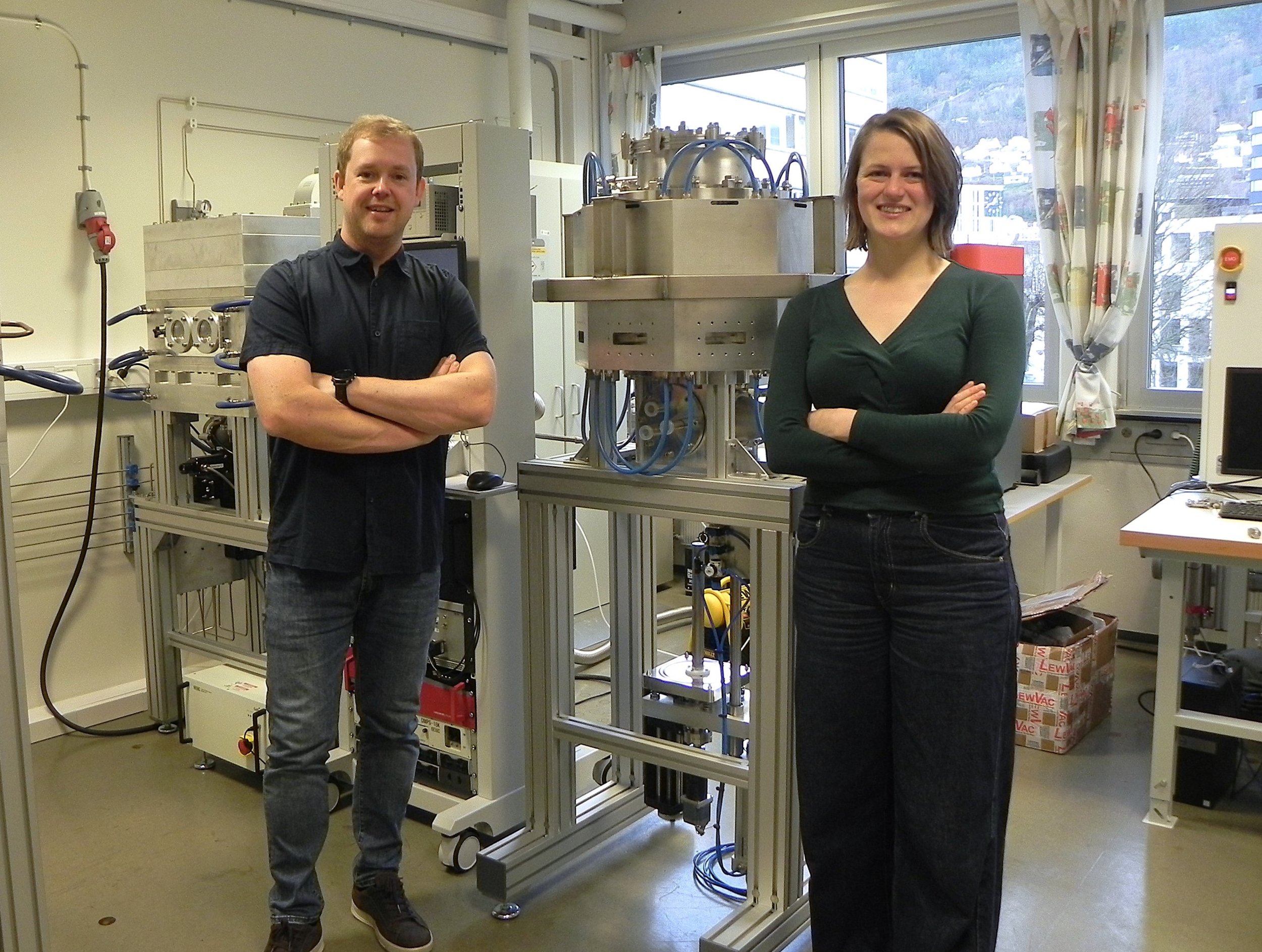
Diamond Wafer Technology at UiB: Justas Zalieckas and Katharina Hauer are developing plasma reactor systems for scalable diamond growth.
Some of the most powerful innovations start with a material the world already knows — but sees in a new way. For physicists Katharina Hauer and Justas Zalieckas at the University of Bergen (UiB), that material is diamond.
Through Diamond Wafer Technology, they are developing plasma reactor systems that could make large, high-quality diamond wafers scalable, affordable, and compatible with industrial standards, opening new opportunities for semiconductors in energy systems, data centers and electric vehicles.
From plasma reactor expertise to diamond growth
– We are two physicists at the University of Bergen working on artificially grown diamond, Katharina says.
Their work is rooted in plasma reactor technology, enabling the synthesis of high-purity diamond under controlled conditions, and at significantly lower temperatures than typical processes.
– Our expertise lies in plasma reactor technology which allows us to grow high-purity diamond for different applications at temperatures as low as 250°C, she explains.
This combination of reactor engineering and advanced materials design makes the project relevant far beyond the lab.
– Our unique and advanced reactor designs allow us to synthesize diamond for fields such as electronics or biomedical implants, Katharina adds.
«Our expertise lies in plasma reactor technology which allows us to grow high-purity diamond… at temperatures as low as 250°C.»
A semiconductor industry reaching Silicon’s limits
The semiconductor industry is currently undergoing major change. New technologies like renewable energy power grids, electric vehicles and data centers place increasing demands on electronic components, and silicon is nearing its physical limits.
– The semiconducting industry is currently undergoing a transition due to fast advancement of new technologies, Katharina says.
– They bring Silicon as material to its limits and alternatives need to be found.
Diamond is one of the strongest candidates.
– Diamond is the best solid semiconductor material known and would be the best alternative, she says.
But despite its exceptional properties, diamond is still not widely used in electronics. Not because the material isn’t good enough, but because scaling production is still too difficult.
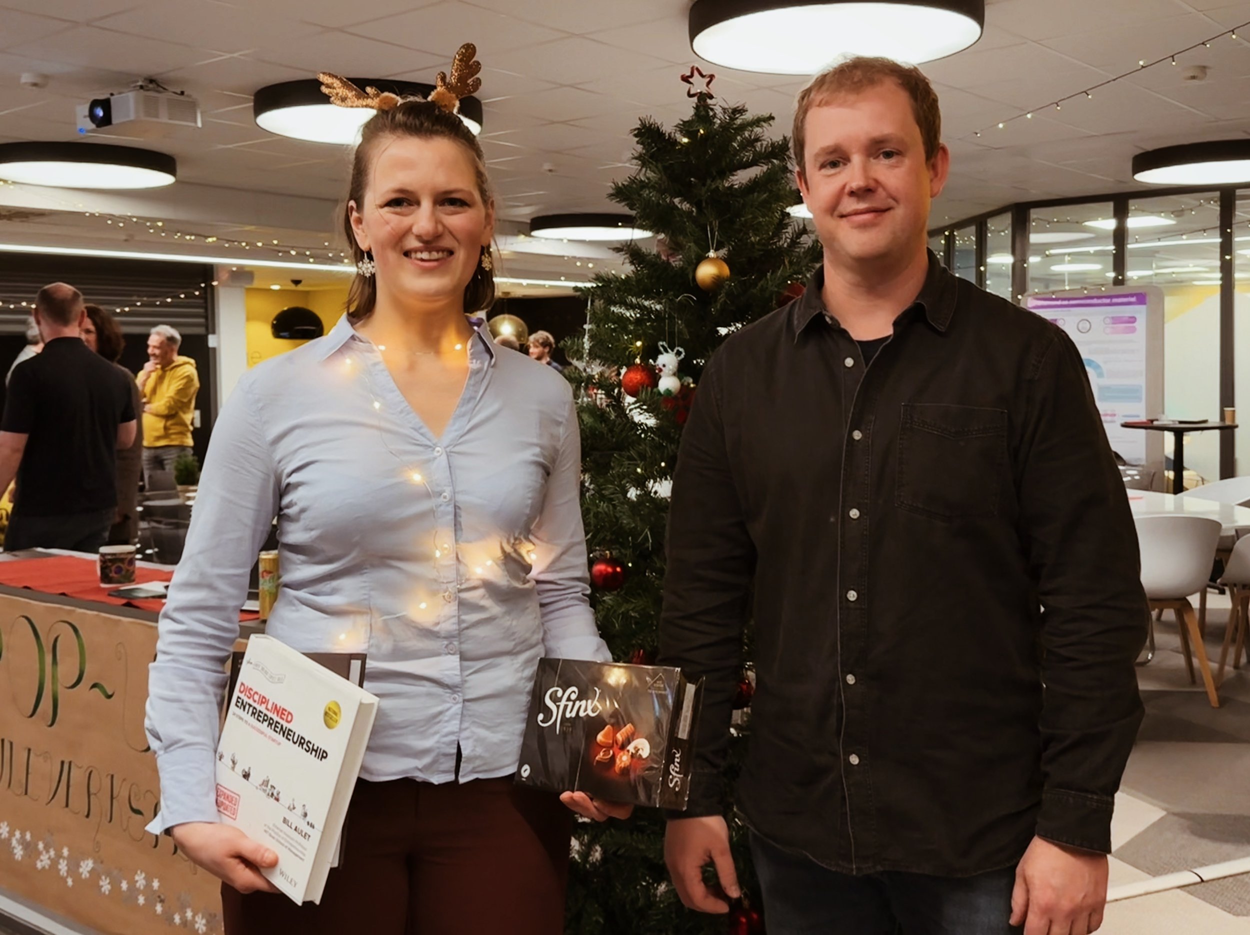
Audience Award winners at the TILT Researcher Christmas Pitch — receiving a signed copy of Disciplined Entrepreneurship by Bill Aulet.
The bottleneck: scaling doesn’t exist
Today, diamond-based electronics struggle to compete with silicon, largely due to cost and scalability.
– Diamond-based electronics producers are not competitive due to low production scalability and high costs, Katharina explains.
– The reason is that the technology for scaling does not exist.
That’s exactly what the project aims to change.
This project seeks to solve a bottleneck in the semiconductor industry: poor heat dissipation in electronics and the inability to manufacture large, high-quality diamond wafers at scale.
«Diamond-based electronics producers are not competitive due to low production scalability and high costs. The reason is that the technology for scaling does not exist.»
A reactor platform to make diamond competitive
Rather than developing diamond materials alone, Diamond Wafer Technology focuses on the manufacturing system — the reactor technology needed to scale.
– We want to enable diamond-based electronics to be competitive and compatible with industry standards with our novel reactor technology, Katharina says.
If successful, their approach could make diamond wafers a realistic option for next-generation electronics, where performance, efficiency and heat management are becoming increasingly critical.
Why TILT and why now
Joining the TILT Researcher Program is part of the team’s plan to build not only technology, but a startup.
– We want to create a startup with our new technology and kickstart with the TILT program, Katharina says.
TILT gives them access to structure, mentoring and an entrepreneurial framework, helping them test use cases, clarify market needs, and explore what it will take to build a company around their reactor platform.
Exploring a completely new technology
The team is still early in the journey, and that is precisely what makes the project exciting.
– This technology is completely new, and we have just begun to explore the applications, Katharina says.
– We are especially excited to see what opportunities will appear in the future.
At the TILT Researcher Christmas Pitch, their momentum was clear: the team won the Audience Award for Best Pitch, receiving a signed copy of Bill Aulet’s Disciplined Entrepreneurship. Katharina also won Best Outfit for bringing holiday spirit to the room; a fitting detail for a project that is pushing a famously hard material into new territory.
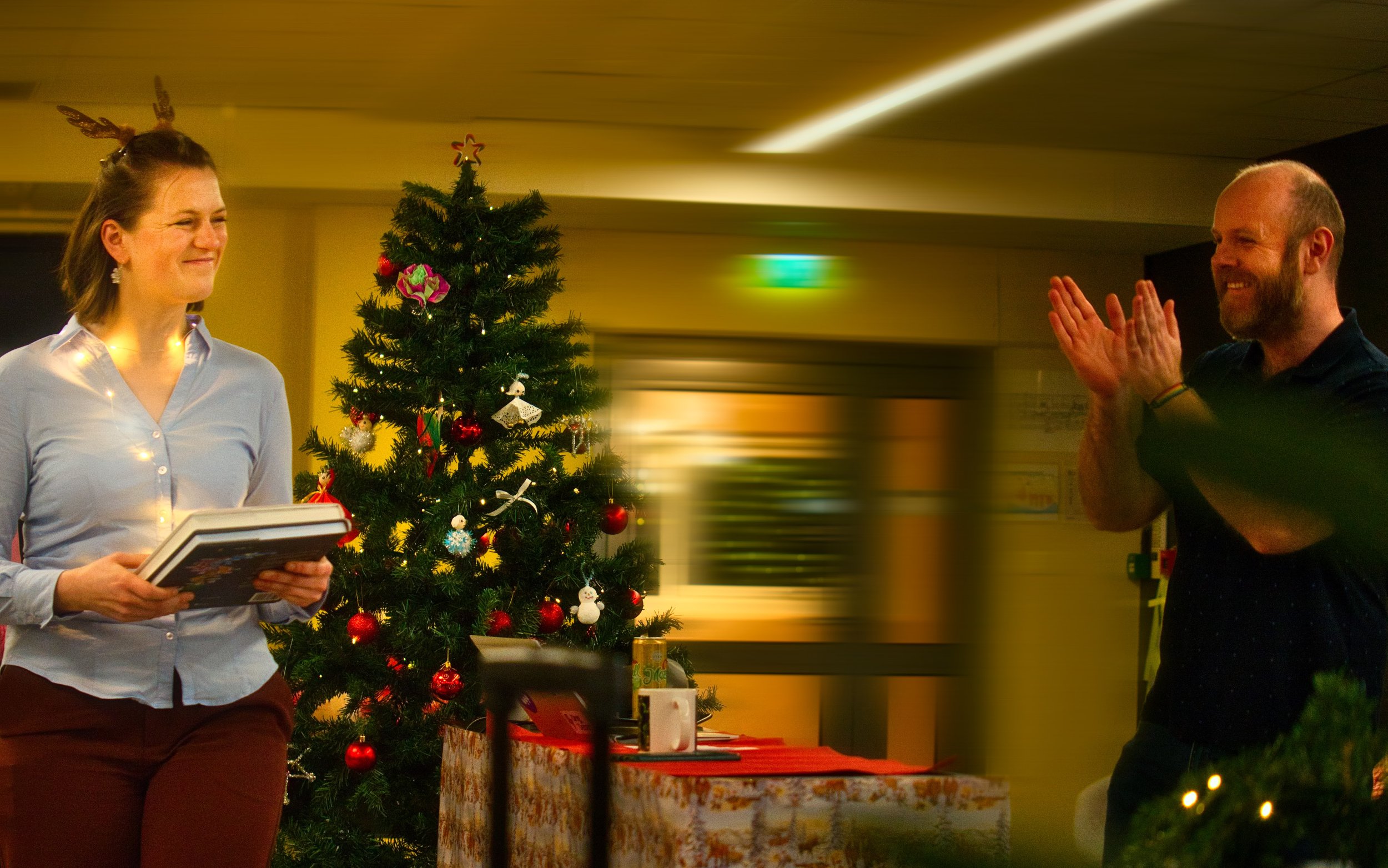
Pitch moment at the TILT Researcher Christmas Pitch, where Katharina won the price for bringing holiday spirit to the room.